| Completion
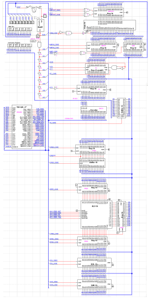
There are 4 buses in my final design. The one between RAM and MBRIN/MAR
doesn't go anywhere. Then there is the "IR BUS" which only branches
out because I wanted a display of the current instruction. Next is the
"Signal Bus" which is the addition I made to simplify the wiring.
Finally, of course there is the main data bus.
The RAM and IR buses are minor and could be easily removed, it is only
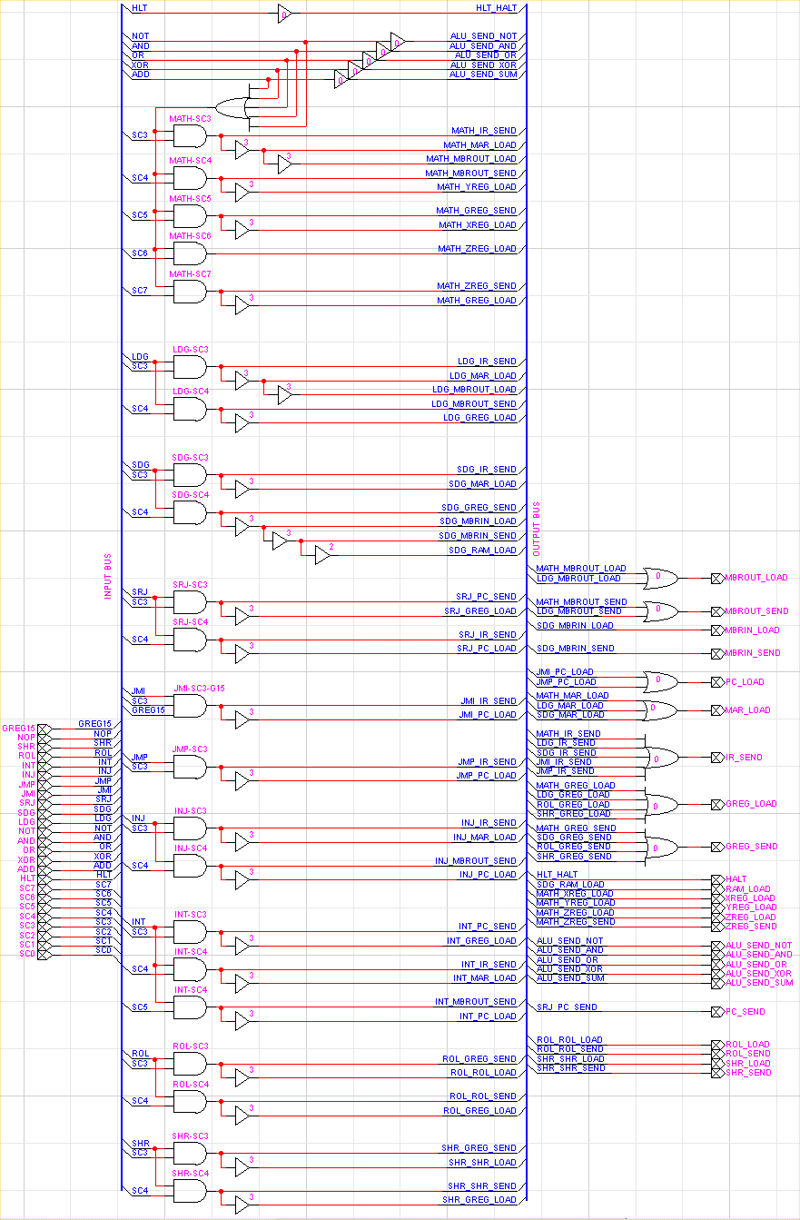
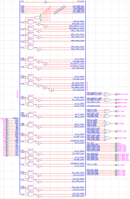
the signal bus and the OpLogic unit that are critical to my design. The
idea is simply that all the wiring for the opcode logic is moved into
a single device that takes in opcode signals and timing signals and outputs
register control signals. This has two benefits.
(1) It vastly simplifies the wiring of the processor as can be seen by
the simplicity of the red wires in the processor diagram.
(2) It presents the actual opcode logic in a very neat format that implicitly
shows the order of actions that are taken. For example, if you click on
the OpLogic diagram below to view the full-scale version and then look
at the LDG actions you will see that they are placed vertically in the
order: ir_send, mar_load, mbrout_load, mbrout_send and greg_load. This
is the order in which the actions occur and the design shows it.
Click either image for a full-scale view.
| Processor |
Operation Logic Unit (OpLogic v7) |
 |
 |
Update: I ran the test program provided by Dr. Hasegawa and was told
my results were correct. I had to make some adjustments to the addresses
because I enter my programs directly into the RAM rather than using a
workbench area with hex keyboards. This was the program I ran:
6009 9008 1010 7010 6000 1012 7000 A000
0000 0120 05A0 0070 0B00 088F 049C FFFF
0000 0000 0001 0000 0000 0000 0000 0000
And this is how it looked after running:
600F 9008 1010 7010 6000 1012 7000 A000
0000 0120 05A0 0070 0B00 088F 049C FFFF
1F5B 0000 0001 0000 0000 0000 0000 0000
back to CAPC...
|