CAPC - Part 8 Supplementary |
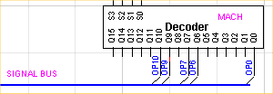
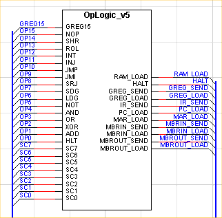
The Operation Logic UnitAs I'm still wasting so much time shifting already built components around to make room for the logic of new opcodes, I've decided to seperate the opcode logic into its own component. Hopefully I'll be able to leave existing layout stuff alone for the most part after this and just concentrate on whatever new stuff I'm adding. My OLU will take in the contents of the signal bus and output the register send/load signals that are pretty much all that the opcode logic ever consists of. I have named this device "OpLogic" and because it gets changed so often it carries a version number. The following diagrams should explain how my new system works. For clarity MBR has been renamed to MBROUT and MBR2 to MBRIN. 1. Opcode signals go onto the signal bus:
2. Opcode signals, clock signals and some miscellaneous signals are carried on the signal bus and given to the OpLogic Unit. The OpLogic Unit processes these signals and outputs register control signals back onto the signal bus:
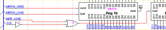
3. Register control signals go out to the registers in the processor:
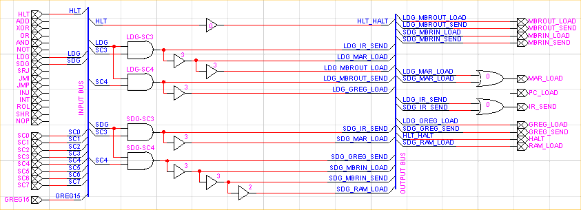
4. Finally, this diagram shows the inside of the OpLogic device in which the HLT, LDG and SDG instructions have been placed:
|