CAPC - Part 4 |
After digging through labs vs chapters amongst the new and
old course material I decided to divide my work up into my own seperations
called parts. Otherwise this would have been lab 5/6 and I don't know
where I lost lab 4.
The LDG InstructionI initially had some trouble understanding the instructions, but since I knew what the goal to this part was I simply wrote it out and then wrote out what I thought the steps were. After that everything fell into place pretty smoothly. Some problems with binary switches were about the worst of it (see the sidebar).
STEPS:
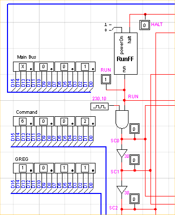
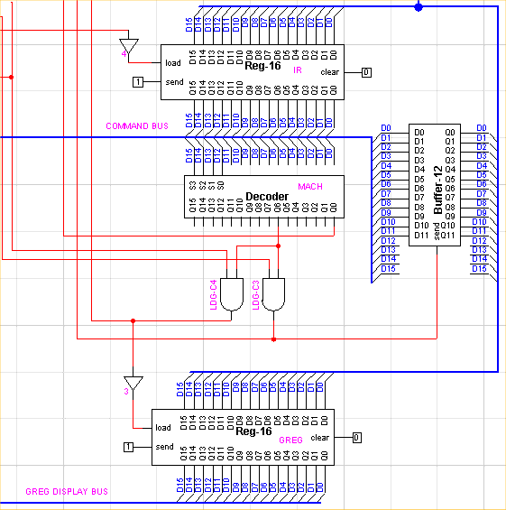
Along the way I added two extra buses and built a sort of I/O console around the power switch for diagnostic purposes. I constructed a 12-bit buffer for holding the address that comes with a giving opcode and placing it on the main bus as necessary. For installing this buffer and wiring the general register into place I made two changes. First, I didn't install a zero register to blank the top 4 bits because I didn't see a reason for it (maybe it's needed later?) Second, I shared the IR output to the decoder and buffer using a bus instead of a messy grid of lines. I already had the bus in place for part of my diagnostic console. It was the "opcode display bus" but I renamed it the "command bus".
back to CAPC... |